1. Crystal Framework and Polytypism of Silicon Carbide
1.1 Cubic and Hexagonal Polytypes: From 3C to 6H and Beyond
(Silicon Carbide Ceramics)
Silicon carbide (SiC) is a covalently adhered ceramic made up of silicon and carbon atoms set up in a tetrahedral control, creating one of the most intricate systems of polytypism in products scientific research.
Unlike many porcelains with a solitary secure crystal framework, SiC exists in over 250 known polytypes– unique piling series of close-packed Si-C bilayers along the c-axis– ranging from cubic 3C-SiC (likewise known as β-SiC) to hexagonal 6H-SiC and rhombohedral 15R-SiC.
The most common polytypes made use of in engineering applications are 3C (cubic), 4H, and 6H (both hexagonal), each showing somewhat different digital band frameworks and thermal conductivities.
3C-SiC, with its zinc blende framework, has the narrowest bandgap (~ 2.3 eV) and is usually grown on silicon substrates for semiconductor gadgets, while 4H-SiC uses superior electron flexibility and is preferred for high-power electronics.
The strong covalent bonding and directional nature of the Si– C bond provide outstanding firmness, thermal security, and resistance to creep and chemical attack, making SiC perfect for extreme setting applications.
1.2 Flaws, Doping, and Digital Properties
Regardless of its structural complexity, SiC can be doped to attain both n-type and p-type conductivity, enabling its usage in semiconductor tools.
Nitrogen and phosphorus act as donor impurities, presenting electrons right into the conduction band, while aluminum and boron act as acceptors, creating openings in the valence band.
However, p-type doping efficiency is restricted by high activation powers, particularly in 4H-SiC, which positions difficulties for bipolar device layout.
Native defects such as screw misplacements, micropipes, and stacking faults can degrade gadget efficiency by functioning as recombination centers or leakage courses, demanding top notch single-crystal growth for digital applications.
The vast bandgap (2.3– 3.3 eV depending on polytype), high break down electrical field (~ 3 MV/cm), and superb thermal conductivity (~ 3– 4 W/m · K for 4H-SiC) make SiC far superior to silicon in high-temperature, high-voltage, and high-frequency power electronics.
2. Handling and Microstructural Design
( Silicon Carbide Ceramics)
2.1 Sintering and Densification Methods
Silicon carbide is naturally tough to densify due to its strong covalent bonding and reduced self-diffusion coefficients, requiring advanced processing approaches to attain full thickness without additives or with marginal sintering aids.
Pressureless sintering of submicron SiC powders is feasible with the enhancement of boron and carbon, which advertise densification by removing oxide layers and enhancing solid-state diffusion.
Warm pushing applies uniaxial pressure throughout heating, enabling full densification at lower temperatures (~ 1800– 2000 ° C )and producing fine-grained, high-strength components appropriate for reducing tools and put on parts.
For large or intricate forms, response bonding is utilized, where permeable carbon preforms are penetrated with molten silicon at ~ 1600 ° C, forming β-SiC in situ with marginal shrinkage.
Nevertheless, recurring free silicon (~ 5– 10%) continues to be in the microstructure, restricting high-temperature efficiency and oxidation resistance above 1300 ° C.
2.2 Additive Manufacturing and Near-Net-Shape Construction
Recent advancements in additive production (AM), specifically binder jetting and stereolithography using SiC powders or preceramic polymers, allow the manufacture of complex geometries formerly unattainable with standard approaches.
In polymer-derived ceramic (PDC) routes, fluid SiC forerunners are formed using 3D printing and afterwards pyrolyzed at heats to generate amorphous or nanocrystalline SiC, often calling for more densification.
These methods reduce machining expenses and product waste, making SiC a lot more obtainable for aerospace, nuclear, and warm exchanger applications where complex designs boost efficiency.
Post-processing actions such as chemical vapor infiltration (CVI) or liquid silicon seepage (LSI) are in some cases made use of to enhance thickness and mechanical stability.
3. Mechanical, Thermal, and Environmental Efficiency
3.1 Stamina, Firmness, and Wear Resistance
Silicon carbide places amongst the hardest recognized materials, with a Mohs solidity of ~ 9.5 and Vickers firmness going beyond 25 GPa, making it extremely immune to abrasion, erosion, and damaging.
Its flexural stamina normally varies from 300 to 600 MPa, depending upon handling technique and grain size, and it maintains toughness at temperature levels approximately 1400 ° C in inert ambiences.
Crack sturdiness, while modest (~ 3– 4 MPa · m ¹/ ²), suffices for lots of structural applications, particularly when incorporated with fiber support in ceramic matrix compounds (CMCs).
SiC-based CMCs are utilized in wind turbine blades, combustor linings, and brake systems, where they use weight savings, gas efficiency, and prolonged service life over metal counterparts.
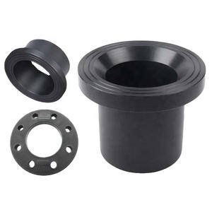
Its exceptional wear resistance makes SiC ideal for seals, bearings, pump components, and ballistic shield, where resilience under harsh mechanical loading is important.
3.2 Thermal Conductivity and Oxidation Stability
One of SiC’s most valuable residential or commercial properties is its high thermal conductivity– as much as 490 W/m · K for single-crystal 4H-SiC and ~ 30– 120 W/m · K for polycrystalline types– surpassing that of many steels and making it possible for reliable heat dissipation.
This residential property is vital in power electronic devices, where SiC tools produce much less waste heat and can operate at higher power densities than silicon-based devices.
At raised temperature levels in oxidizing environments, SiC forms a safety silica (SiO ₂) layer that slows more oxidation, giving great environmental toughness approximately ~ 1600 ° C.
However, in water vapor-rich atmospheres, this layer can volatilize as Si(OH)₄, bring about sped up destruction– a key obstacle in gas wind turbine applications.
4. Advanced Applications in Power, Electronic Devices, and Aerospace
4.1 Power Electronic Devices and Semiconductor Devices
Silicon carbide has actually reinvented power electronics by allowing gadgets such as Schottky diodes, MOSFETs, and JFETs that run at greater voltages, frequencies, and temperature levels than silicon matchings.
These tools reduce energy losses in electric cars, renewable energy inverters, and commercial motor drives, adding to worldwide power efficiency enhancements.
The capability to operate at junction temperature levels over 200 ° C allows for streamlined cooling systems and raised system integrity.
Furthermore, SiC wafers are utilized as substratums for gallium nitride (GaN) epitaxy in high-electron-mobility transistors (HEMTs), integrating the advantages of both wide-bandgap semiconductors.
4.2 Nuclear, Aerospace, and Optical Solutions
In nuclear reactors, SiC is a crucial element of accident-tolerant fuel cladding, where its low neutron absorption cross-section, radiation resistance, and high-temperature toughness boost safety and security and performance.
In aerospace, SiC fiber-reinforced composites are used in jet engines and hypersonic cars for their lightweight and thermal security.
Additionally, ultra-smooth SiC mirrors are employed in space telescopes due to their high stiffness-to-density proportion, thermal stability, and polishability to sub-nanometer roughness.
In summary, silicon carbide porcelains represent a foundation of modern-day advanced products, integrating outstanding mechanical, thermal, and digital properties.
Through accurate control of polytype, microstructure, and processing, SiC continues to make it possible for technical breakthroughs in power, transportation, and severe environment engineering.
5. Supplier
TRUNNANO is a supplier of Spherical Tungsten Powder with over 12 years of experience in nano-building energy conservation and nanotechnology development. It accepts payment via Credit Card, T/T, West Union and Paypal. Trunnano will ship the goods to customers overseas through FedEx, DHL, by air, or by sea. If you want to know more about Spherical Tungsten Powder, please feel free to contact us and send an inquiry(sales5@nanotrun.com).
Tags: silicon carbide ceramic,silicon carbide ceramic products, industry ceramic
All articles and pictures are from the Internet. If there are any copyright issues, please contact us in time to delete.
Inquiry us