1. Material Fundamentals and Structural Attributes of Alumina Ceramics
1.1 Crystallographic and Compositional Basis of α-Alumina
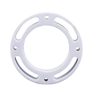
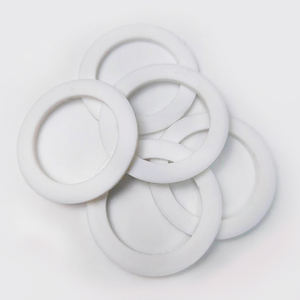
(Alumina Ceramic Substrates)
Alumina ceramic substrates, primarily composed of light weight aluminum oxide (Al ₂ O ₃), function as the backbone of contemporary electronic packaging because of their outstanding equilibrium of electrical insulation, thermal stability, mechanical toughness, and manufacturability.
One of the most thermodynamically secure phase of alumina at high temperatures is corundum, or α-Al Two O FIVE, which takes shape in a hexagonal close-packed oxygen lattice with light weight aluminum ions occupying two-thirds of the octahedral interstitial websites.
This thick atomic setup conveys high hardness (Mohs 9), outstanding wear resistance, and strong chemical inertness, making α-alumina appropriate for rough operating atmospheres.
Industrial substrates usually have 90– 99.8% Al Two O THREE, with small enhancements of silica (SiO TWO), magnesia (MgO), or unusual planet oxides used as sintering help to promote densification and control grain development during high-temperature processing.
Greater purity grades (e.g., 99.5% and above) display exceptional electric resistivity and thermal conductivity, while reduced purity variations (90– 96%) use cost-effective services for less demanding applications.
1.2 Microstructure and Defect Engineering for Electronic Dependability
The efficiency of alumina substratums in electronic systems is seriously based on microstructural harmony and issue reduction.
A penalty, equiaxed grain structure– generally varying from 1 to 10 micrometers– ensures mechanical honesty and decreases the likelihood of fracture breeding under thermal or mechanical stress.
Porosity, particularly interconnected or surface-connected pores, should be reduced as it weakens both mechanical strength and dielectric performance.
Advanced processing techniques such as tape casting, isostatic pushing, and regulated sintering in air or controlled atmospheres make it possible for the production of substrates with near-theoretical density (> 99.5%) and surface area roughness listed below 0.5 µm, necessary for thin-film metallization and cord bonding.
Additionally, pollutant segregation at grain limits can lead to leak currents or electrochemical migration under prejudice, demanding rigorous control over raw material pureness and sintering conditions to ensure long-term dependability in humid or high-voltage environments.
2. Manufacturing Processes and Substrate Construction Technologies
( Alumina Ceramic Substrates)
2.1 Tape Spreading and Eco-friendly Body Handling
The manufacturing of alumina ceramic substrates starts with the prep work of a highly distributed slurry consisting of submicron Al two O three powder, organic binders, plasticizers, dispersants, and solvents.
This slurry is refined using tape spreading– a continual technique where the suspension is spread over a relocating service provider movie using a precision medical professional blade to achieve uniform density, commonly in between 0.1 mm and 1.0 mm.
After solvent dissipation, the resulting “eco-friendly tape” is flexible and can be punched, drilled, or laser-cut to form using openings for vertical affiliations.
Numerous layers might be laminated to produce multilayer substrates for intricate circuit combination, although the majority of industrial applications make use of single-layer configurations due to set you back and thermal growth considerations.
The environment-friendly tapes are after that very carefully debound to eliminate organic additives with managed thermal decay before final sintering.
2.2 Sintering and Metallization for Circuit Combination
Sintering is carried out in air at temperature levels in between 1550 ° C and 1650 ° C, where solid-state diffusion drives pore removal and grain coarsening to attain complete densification.
The straight contraction during sintering– typically 15– 20%– have to be precisely predicted and made up for in the design of green tapes to ensure dimensional accuracy of the last substratum.
Adhering to sintering, metallization is put on form conductive traces, pads, and vias.
Two key techniques control: thick-film printing and thin-film deposition.
In thick-film technology, pastes including metal powders (e.g., tungsten, molybdenum, or silver-palladium alloys) are screen-printed onto the substrate and co-fired in a decreasing atmosphere to develop durable, high-adhesion conductors.
For high-density or high-frequency applications, thin-film procedures such as sputtering or evaporation are made use of to deposit bond layers (e.g., titanium or chromium) complied with by copper or gold, making it possible for sub-micron pattern via photolithography.
Vias are full of conductive pastes and fired to develop electrical interconnections in between layers in multilayer styles.
3. Useful Qualities and Performance Metrics in Electronic Solution
3.1 Thermal and Electrical Actions Under Functional Stress
Alumina substrates are treasured for their desirable combination of moderate thermal conductivity (20– 35 W/m · K for 96– 99.8% Al ₂ O ₃), which allows efficient warm dissipation from power devices, and high quantity resistivity (> 10 ¹⁴ Ω · cm), making certain marginal leakage current.
Their dielectric consistent (εᵣ ≈ 9– 10 at 1 MHz) is steady over a wide temperature level and regularity variety, making them suitable for high-frequency circuits up to several gigahertz, although lower-κ products like aluminum nitride are liked for mm-wave applications.
The coefficient of thermal development (CTE) of alumina (~ 6.8– 7.2 ppm/K) is sensibly well-matched to that of silicon (~ 3 ppm/K) and specific product packaging alloys, decreasing thermo-mechanical anxiety during gadget procedure and thermal biking.
Nonetheless, the CTE inequality with silicon remains a concern in flip-chip and direct die-attach setups, commonly needing certified interposers or underfill materials to minimize tiredness failure.
3.2 Mechanical Effectiveness and Ecological Toughness
Mechanically, alumina substratums show high flexural stamina (300– 400 MPa) and excellent dimensional security under tons, enabling their use in ruggedized electronic devices for aerospace, automotive, and industrial control systems.
They are immune to resonance, shock, and creep at raised temperatures, keeping architectural integrity as much as 1500 ° C in inert atmospheres.
In moist environments, high-purity alumina shows minimal wetness absorption and excellent resistance to ion movement, guaranteeing long-lasting dependability in outdoor and high-humidity applications.
Surface firmness likewise secures against mechanical damage during handling and setting up, although care needs to be required to avoid side breaking because of inherent brittleness.
4. Industrial Applications and Technological Impact Throughout Sectors
4.1 Power Electronic Devices, RF Modules, and Automotive Solutions
Alumina ceramic substrates are common in power electronic components, consisting of shielded gate bipolar transistors (IGBTs), MOSFETs, and rectifiers, where they offer electrical isolation while promoting heat transfer to warmth sinks.
In radio frequency (RF) and microwave circuits, they serve as carrier systems for hybrid incorporated circuits (HICs), surface acoustic wave (SAW) filters, and antenna feed networks because of their secure dielectric residential properties and reduced loss tangent.
In the automobile industry, alumina substratums are utilized in engine control units (ECUs), sensing unit packages, and electrical car (EV) power converters, where they withstand heats, thermal cycling, and exposure to destructive fluids.
Their dependability under extreme conditions makes them crucial for safety-critical systems such as anti-lock stopping (ABDOMINAL) and progressed driver help systems (ADAS).
4.2 Clinical Gadgets, Aerospace, and Emerging Micro-Electro-Mechanical Equipments
Past consumer and commercial electronics, alumina substrates are employed in implantable medical tools such as pacemakers and neurostimulators, where hermetic securing and biocompatibility are paramount.
In aerospace and defense, they are utilized in avionics, radar systems, and satellite communication modules due to their radiation resistance and stability in vacuum environments.
Additionally, alumina is significantly utilized as a structural and protecting system in micro-electro-mechanical systems (MEMS), consisting of stress sensing units, accelerometers, and microfluidic devices, where its chemical inertness and compatibility with thin-film processing are advantageous.
As digital systems remain to require higher power thickness, miniaturization, and dependability under extreme problems, alumina ceramic substrates remain a foundation material, bridging the gap between performance, expense, and manufacturability in sophisticated electronic packaging.
5. Provider
Alumina Technology Co., Ltd focus on the research and development, production and sales of aluminum oxide powder, aluminum oxide products, aluminum oxide crucible, etc., serving the electronics, ceramics, chemical and other industries. Since its establishment in 2005, the company has been committed to providing customers with the best products and services. If you are looking for high quality alumina technology, please feel free to contact us. (nanotrun@yahoo.com)
Tags: Alumina Ceramic Substrates, Alumina Ceramics, alumina
All articles and pictures are from the Internet. If there are any copyright issues, please contact us in time to delete.
Inquiry us