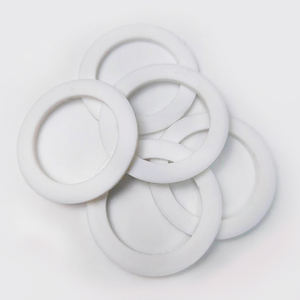
1. Product Fundamentals and Structural Characteristics of Alumina Ceramics
1.1 Crystallographic and Compositional Basis of α-Alumina
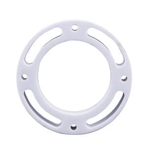
(Alumina Ceramic Substrates)
Alumina ceramic substratums, mainly composed of light weight aluminum oxide (Al ₂ O SIX), work as the foundation of modern-day electronic packaging because of their outstanding balance of electrical insulation, thermal stability, mechanical toughness, and manufacturability.
One of the most thermodynamically steady phase of alumina at high temperatures is diamond, or α-Al ₂ O THREE, which takes shape in a hexagonal close-packed oxygen lattice with light weight aluminum ions occupying two-thirds of the octahedral interstitial sites.
This thick atomic arrangement conveys high hardness (Mohs 9), outstanding wear resistance, and solid chemical inertness, making α-alumina ideal for rough operating environments.
Business substrates normally contain 90– 99.8% Al Two O THREE, with minor additions of silica (SiO TWO), magnesia (MgO), or unusual planet oxides used as sintering aids to promote densification and control grain growth throughout high-temperature handling.
Higher pureness qualities (e.g., 99.5% and over) exhibit premium electric resistivity and thermal conductivity, while lower purity variations (90– 96%) provide cost-effective remedies for less demanding applications.
1.2 Microstructure and Defect Engineering for Electronic Reliability
The efficiency of alumina substrates in electronic systems is critically dependent on microstructural harmony and issue minimization.
A penalty, equiaxed grain structure– usually ranging from 1 to 10 micrometers– guarantees mechanical stability and decreases the likelihood of split proliferation under thermal or mechanical tension.
Porosity, especially interconnected or surface-connected pores, must be minimized as it degrades both mechanical strength and dielectric performance.
Advanced handling strategies such as tape casting, isostatic pushing, and regulated sintering in air or managed atmospheres make it possible for the production of substrates with near-theoretical thickness (> 99.5%) and surface roughness below 0.5 µm, important for thin-film metallization and cable bonding.
In addition, pollutant partition at grain boundaries can result in leakage currents or electrochemical migration under predisposition, necessitating rigorous control over raw material pureness and sintering conditions to ensure long-lasting reliability in humid or high-voltage environments.
2. Manufacturing Processes and Substratum Construction Technologies
( Alumina Ceramic Substrates)
2.1 Tape Casting and Eco-friendly Body Processing
The manufacturing of alumina ceramic substrates starts with the preparation of a highly distributed slurry including submicron Al ₂ O two powder, organic binders, plasticizers, dispersants, and solvents.
This slurry is refined via tape casting– a continual method where the suspension is topped a relocating carrier film using an accuracy physician blade to accomplish uniform density, commonly between 0.1 mm and 1.0 mm.
After solvent evaporation, the resulting “green tape” is flexible and can be punched, pierced, or laser-cut to develop by means of openings for upright interconnections.
Several layers may be laminated flooring to develop multilayer substratums for complicated circuit combination, although most of commercial applications utilize single-layer configurations due to cost and thermal growth considerations.
The environment-friendly tapes are then thoroughly debound to eliminate organic additives via regulated thermal decomposition prior to final sintering.
2.2 Sintering and Metallization for Circuit Assimilation
Sintering is performed in air at temperatures between 1550 ° C and 1650 ° C, where solid-state diffusion drives pore removal and grain coarsening to accomplish complete densification.
The direct contraction during sintering– generally 15– 20%– have to be precisely forecasted and made up for in the style of green tapes to make certain dimensional precision of the final substratum.
Complying with sintering, metallization is related to form conductive traces, pads, and vias.
2 key techniques control: thick-film printing and thin-film deposition.
In thick-film modern technology, pastes consisting of steel powders (e.g., tungsten, molybdenum, or silver-palladium alloys) are screen-printed onto the substratum and co-fired in a decreasing environment to create robust, high-adhesion conductors.
For high-density or high-frequency applications, thin-film procedures such as sputtering or dissipation are made use of to deposit adhesion layers (e.g., titanium or chromium) complied with by copper or gold, making it possible for sub-micron pattern using photolithography.
Vias are filled with conductive pastes and terminated to develop electric affiliations between layers in multilayer layouts.
3. Practical Features and Performance Metrics in Electronic Solution
3.1 Thermal and Electrical Habits Under Operational Stress
Alumina substratums are valued for their favorable combination of modest thermal conductivity (20– 35 W/m · K for 96– 99.8% Al ₂ O SIX), which enables effective heat dissipation from power devices, and high volume resistivity (> 10 ¹⁴ Ω · centimeters), ensuring marginal leakage current.
Their dielectric consistent (εᵣ ≈ 9– 10 at 1 MHz) is stable over a broad temperature level and regularity array, making them suitable for high-frequency circuits as much as a number of gigahertz, although lower-κ materials like aluminum nitride are liked for mm-wave applications.
The coefficient of thermal development (CTE) of alumina (~ 6.8– 7.2 ppm/K) is reasonably well-matched to that of silicon (~ 3 ppm/K) and certain packaging alloys, reducing thermo-mechanical stress during device operation and thermal biking.
Nevertheless, the CTE mismatch with silicon stays an issue in flip-chip and straight die-attach arrangements, typically calling for compliant interposers or underfill materials to mitigate fatigue failure.
3.2 Mechanical Robustness and Ecological Durability
Mechanically, alumina substrates exhibit high flexural toughness (300– 400 MPa) and exceptional dimensional stability under tons, enabling their usage in ruggedized electronics for aerospace, automobile, and industrial control systems.
They are immune to vibration, shock, and creep at elevated temperature levels, preserving structural honesty as much as 1500 ° C in inert ambiences.
In moist settings, high-purity alumina shows minimal dampness absorption and superb resistance to ion movement, ensuring lasting reliability in outdoor and high-humidity applications.
Surface firmness additionally safeguards against mechanical damage during handling and assembly, although care needs to be required to stay clear of side damaging due to fundamental brittleness.
4. Industrial Applications and Technical Influence Throughout Sectors
4.1 Power Electronics, RF Modules, and Automotive Equipments
Alumina ceramic substrates are common in power digital modules, consisting of protected entrance bipolar transistors (IGBTs), MOSFETs, and rectifiers, where they provide electric isolation while promoting warm transfer to warmth sinks.
In superhigh frequency (RF) and microwave circuits, they function as service provider platforms for crossbreed incorporated circuits (HICs), surface area acoustic wave (SAW) filters, and antenna feed networks because of their steady dielectric residential or commercial properties and reduced loss tangent.
In the vehicle industry, alumina substrates are utilized in engine control units (ECUs), sensor bundles, and electric car (EV) power converters, where they endure heats, thermal biking, and exposure to harsh liquids.
Their integrity under rough problems makes them essential for safety-critical systems such as anti-lock braking (ABS) and advanced vehicle driver aid systems (ADAS).
4.2 Clinical Gadgets, Aerospace, and Arising Micro-Electro-Mechanical Equipments
Past consumer and industrial electronics, alumina substrates are employed in implantable clinical tools such as pacemakers and neurostimulators, where hermetic sealing and biocompatibility are paramount.
In aerospace and defense, they are used in avionics, radar systems, and satellite interaction components as a result of their radiation resistance and security in vacuum settings.
Furthermore, alumina is increasingly used as an architectural and protecting system in micro-electro-mechanical systems (MEMS), including pressure sensing units, accelerometers, and microfluidic gadgets, where its chemical inertness and compatibility with thin-film processing are helpful.
As digital systems continue to demand higher power densities, miniaturization, and reliability under extreme conditions, alumina ceramic substratums stay a foundation product, connecting the space in between efficiency, price, and manufacturability in sophisticated digital packaging.
5. Supplier
Alumina Technology Co., Ltd focus on the research and development, production and sales of aluminum oxide powder, aluminum oxide products, aluminum oxide crucible, etc., serving the electronics, ceramics, chemical and other industries. Since its establishment in 2005, the company has been committed to providing customers with the best products and services. If you are looking for high quality alumina technology, please feel free to contact us. (nanotrun@yahoo.com)
Tags: Alumina Ceramic Substrates, Alumina Ceramics, alumina
All articles and pictures are from the Internet. If there are any copyright issues, please contact us in time to delete.
Inquiry us